Cache Memories
Paper 1
The paper describes an analytical model for the access and cycle times of on-chip direct-mapped and set-associative caches. The paper is an extension of [1], Wada et al's access time model. The authors have included many new features like models for tag array, comparator and multiplexer drivers, nonstep stage input slopes, rectangular stacking of memory subarrays, a transistor-level decoder model, column-multiplexed bitlines controlled by an additional array organizational parameter, load dependent size transistors for wordline drivers, and output of cycle times as well as access times. These enhancements are first used to modify the cache structure to closely represent a real cache, and secondly, using modeling techniques to estimate delay.
Observation
The decoder first decodes the address and selects the appropriate row by driving one wordline in the data array and tag array. The value stored in the memory cell determines which bitline goes low.
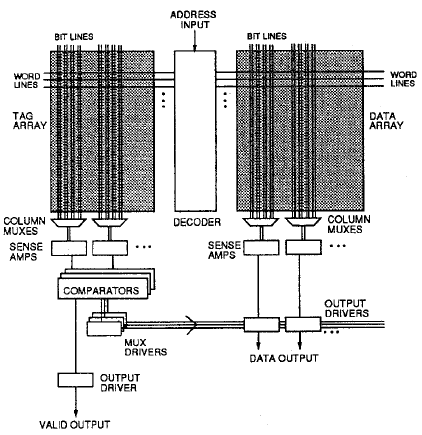
Fig 1
Fig 1 shows the organization of the cache being considered. The address decoded by the decoder selects in tag array and data array an appropriate row enabling the word line by driving it high (which is the same word line for both data and tag array). There are memory cells in each row. Each memory cell is associated with a pair of bit lines. The bitlines are initially precharged to high. Then depending on the value stored in each memory cell, the corresponding wordline goes low. There are sense amplifiers that monitor a pair of bitlines that detects any change in value. Since the sense amplifiers are shared among several pairs of bitlines (usually one sense amplifier for a word or group, of bitlines, depending on the layout parameters), there is a multiplexer before sense amplifier. The lines of the multiplexer are driven by the decoder.
The data from the tag array is compared with the tag bits of the address. The output of the comparison is hit/miss which is the valid output as shown in fig and is used to drive the output multiplexers. The output multiplexer selects the appropriate data from data array.
The authors have almost the same array organization parameters as Wada. The parameters are C, B, A, S. Where C is the Cache size, B is the Block size, A is the associativity, S is the number of sets (S = C/(B . A)). The authors have argued that Wada model has one problem. Wada et al had suggested how the array can be broken down horizontally or vertically by defining two parameters Ndwl and Ndbl (Ndwl is the number of segments per word line of data array and Ndbl is the number of segments per bit line of bit array). The organization is larger in one direction. To overcome this, they have suggested adding another organization parameter called Nspd which is number of sets mapped to a word line. Depending on the Cache and block size, the optimum values of the Ndwl, Ndbl, Nspd are calculated. The tag array can also be configured the same way.
The delays are calculated for the following components
- Decoder
- Word lines
- Bit lines
- Sense amplifiers
- Comparators
- Multiplexor drivers
- Output drivers.
The delay is calculated for both data and tag arrays. Each component is decomposed into several equivalent RC circuits to calculate the delay.
First the resistances and capacitances of each component is calculated. After which the delay of each component is calculated by stages.
After calculating the delays, the total access time and cycle times are calculated. To calculate the access time the authors have considered two critical paths. First, when the delay to read the tag array is more than data array. This is usually when the tag array has to perform the comparism and drive the multiplexer select lines. Second, when the delay to read the data array is more than tag array. Both of them should be considered when designing a cache.
The cycle times vary based on the circuit techniques. It is usually larger than access time if it is a pipelined or post charge circuit. The authors have assumed that the cycle time is access time plus the precharge. This is because they have assumed a conventional model. The elements that are assumed to be precharged are the decoders, the bitlines and the comparator. The authors have assumed the maximum delay to be the time when the wordline goes low and bitline goes high and is the prominent delay. Thus they calculate the cycle time.
How the new technique is verified
The authors have shown the effect of cache size, block size and associativity on the access and cycle times. They have assumed the output width to be 64 bits and 32 address bits.
By varying the cache size the authors have shown the affects of cache size on cache access and cycle times. The optimum array organization parameters are found by varying the Ndwl, Ndbl, Nspd. The corresponding access and cycle times were found and plotted. From the author has shown that comparator is responsible for the significant portion the access time and that the tag side is always the critical path.
Similarly the access times and cycle times are calculated as a function of the block size. For a direct mapped cache the access and cycle times dropped as the block size increased. Most of this is due to the decrease in decoder delay. But in a set associative case, the access and cycle times increase as the block size increases. This is due to the increased loading at the outputs of the drivers.
Finally, the authors have shown the effect of associativity on the access and cycle times. As the associativity increases the access and cycle time increase dramatically.
Conclusion
The authors have designed a cache which is different from the previous model presented by Wada et al there by designing a cache model which is more closer to real on chip cache memories.
I feel that the authors have not discussed in much detail about the effects of associativity. The hit and miss rates are important in designing a cache. The hit or miss rates is dependant on associativity also. The authors have mainly focused on the access and cycle times.
References:
1. T. Wada, S. Rajan, and S. A. Przybylski, “An analytical access time model for on-chip cache memories,” IEEE J. Solid-State Circuits, vol.27, pp. 1147-1156, Aug. 1992.
2. Mark D. Hill, Alan Jay Smith, "Evaluating Associativity in CPU Caches", IEEE Transactions on Computers, Vol. 38, pp 1612-1630, December 1989